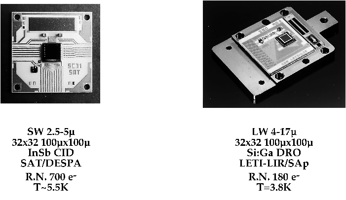
For the short wavelength channel, the detector array was an InSb 32
![]() 32 pixels Charge Injection Device (CID), manufactured by
the Société Anonyme des Télécommunications. At the time of
the ESA Call for `Proposals for ISO instruments', it was already
qualified and offered the advantages of a low operating
temperature and a large radiation tolerance, compatible with the
ISO mission, including the 89% filling factor of the
100
32 pixels Charge Injection Device (CID), manufactured by
the Société Anonyme des Télécommunications. At the time of
the ESA Call for `Proposals for ISO instruments', it was already
qualified and offered the advantages of a low operating
temperature and a large radiation tolerance, compatible with the
ISO mission, including the 89% filling factor of the
100![]() 100
100![]() m
m![]() pixels and the charge injection
efficiency. The effective quantum efficiency was 0.3 at 4
pixels and the charge injection
efficiency. The effective quantum efficiency was 0.3 at 4![]() m,
with a flat curve towards shorter wavelengths, and a cut-off
at 5.2
m,
with a flat curve towards shorter wavelengths, and a cut-off
at 5.2![]() m.
m.
Hybrid electronics for control and readout were designed to work at 4 K, close to the chip. The array and its cold electronics were housed behind a titanium cover which provided a shield against cosmic ray particles and straylight.
The readout of the SW array was an elaborated form of CID readout.
Measurement of the pixel charges was done by sensing the voltages
of the 32 output lines after sequentially injecting the pixel
charges into the substrate through column voltage gates. The analogue
chain used an adaptive filter followed by a high gain preamplifier.
The filtering scheme gave a periodic signal with 32 peaks
corresponding to the pixel intensities. The baseline was measured
before and after each injection, giving 65 measurements. The true
value of the pixel charge was provided by the difference between the
peak measurement and the mean value between the 2 adjacent
baseline measurements. This scheme held for the 32 photosensitive
lines, and also for 2 blind reference lines used for removing the
correlated pick-up noise. The data were stored in a ![]() frame for the baseline measurements, and a
frame for the baseline measurements, and a ![]() frame for
the peak measurements. The allowed integration times were:
0.28 s, 2 s, 6 s, 20 s and 60 s.
frame for
the peak measurements. The allowed integration times were:
0.28 s, 2 s, 6 s, 20 s and 60 s.
The array was little affected by charge particle induced glitches, therefore long integration times were practical. Long on-chip integration times reduced the impact of the high readout noise of this device.
There were three possible readout modes:
When the integration time was 0.28 seconds, four images were averaged on board before downlink as the telemetry rate only allowed to send one image every second.
The noise on the SW channel had several origins: detector noise, amplifier noise, electrical cross-talk and pick-up noise.
The output signal was very small, a few mV, and the lines were very easily affected by pick-up noise. To reduce the impact of this noise source, the signals from the 2 blind lines (see Section 2.3.1) went through the electronic chain as if they were pixel lines. They were used as a reference for the correlated pick-up noise. A correlation matrix between the pixels on the reference lines and the actual pixels was used to remove the correlated noise.
Cross-talk between pixels arose in the connecting wires
between the array and the cold electronics. Since odd and even lines
had geometrically separated outputs, the cross-talk had a strong
parity characteristic. Echoes of a bright source on line ![]() were found
on lines
were found
on lines ![]() and
and ![]() , but not on lines
, but not on lines ![]() and
and ![]() . A cross-talk
matrix was used in the data processing (see Section 5.5.1)
to remove this effect.
. A cross-talk
matrix was used in the data processing (see Section 5.5.1)
to remove this effect.
After removal of the correlated noise and of the electrical cross-talk, the
remaining noise can be very well modelled by a constant readout
noise and the photon shot noise. The readout noise was about 700
![]() /pixel rms.
/pixel rms.
The SW array, like every CID, was non-linear. Deviation from linearity
reached 20% at 2/3 of the dynamic range. The device saturated at
![]() .
.
The Analogue to Digital Converter (ADC), and the programmable offset and
gain controls were shared by the SW and the LW channels. For the SW channel,
the offset was
automatically set and the gain was 2. This setting of the gain
was recommended, to provide a good sampling of the
noise, while preserving the whole dynamic range of the array. In these
conditions, one Analogue to Digital Unit (ADU) corresponded
to 360 e![]() , the pixel saturated at 3000 ADU, and the noise was 2 ADU
rms.
, the pixel saturated at 3000 ADU, and the noise was 2 ADU
rms.
Four pixels remained throughout the mission at a high readout signal and did not provide any useful information. The positions of these pixels are given in the CCGSWDEAD calibration file (see Section 6.1.1).