At the time of the ESA Call for `Proposals for ISO instruments',
there was no array available in Europe suitable for usage in the long
wavelength channel of ISOCAM. A specific development programme was
undertaken at the Laboratoire
d'imagerie Infrarouge (CEA/LETI) in Grenoble. It led to a 32 ![]() 32
gallium doped silicon photoconductor array hybridized by indium
bumps to a direct voltage readout circuit. The pixel pitch was 100
32
gallium doped silicon photoconductor array hybridized by indium
bumps to a direct voltage readout circuit. The pixel pitch was 100![]() m
and the detectors were 500
m
and the detectors were 500![]() m thick. A 25 V bias
voltage was applied to the photoconductor, providing the optimum
trade-off between responsivity and the overhead required to allow for
stabilisation of detector response. With
this bias voltage, the responsivity at 15
m thick. A 25 V bias
voltage was applied to the photoconductor, providing the optimum
trade-off between responsivity and the overhead required to allow for
stabilisation of detector response. With
this bias voltage, the responsivity at 15![]() m was 10
m was 10![]() V/W,
corresponding to a photoconductive-gain
V/W,
corresponding to a photoconductive-gain ![]() quantum
efficiency product of
quantum
efficiency product of ![]()
![]()
![]()
![]() 1.
To a first approximation,
at shorter wavelengths, the responsivity decreased with
1.
To a first approximation,
at shorter wavelengths, the responsivity decreased with
![]() , and there was a long wavelength cut-off at 18
, and there was a long wavelength cut-off at 18![]() m.
m.
To obtain a 100% filling factor, the front surface was doped to ensure
a good electrical surface conductivity and the bias voltage was applied
to an aluminum frame on the side of the optically sensitive area. An
external guard, 3 pixels wide, was added around the 32 ![]() 32
sensitive pixel frame to prevent field line distortion in the detectors
at the edges. The cross-talk was very low, and remained below
1.5%, even for the 12
32
sensitive pixel frame to prevent field line distortion in the detectors
at the edges. The cross-talk was very low, and remained below
1.5%, even for the 12
![]() pfov which had the fastest
lens of the camera (numerical aperture
pfov which had the fastest
lens of the camera (numerical aperture ![]() f/1).
f/1).
For each pixel, the readout circuit had an integration capacitance
of 0.12 pF and a MOSFET follower stage with a gain of 0.8.
A double-sampling readout scheme was used, first
resetting the output capacitance and measuring this reset level,
then integrating and measuring the level at the end of the
integration. The reset level and end of integration level were stored and
transmitted to the ground in two separate 32 ![]() 32 frames. The
integration times allowed were: 0.28 s, 2 s, 5 s, 10 s, or 20 s.
32 frames. The
integration times allowed were: 0.28 s, 2 s, 5 s, 10 s, or 20 s.
As for the SW detector there were three different readout modes:
When the on-chip integration time was 0.28 seconds, four images were averaged on board before being downlinked as the telemetry rate only supported downlinking of one image every second. Only for special calibration measurements was the sampled mode used with 0.28 seconds integration time, in order to get a higher time resolution than in the accumulated mode. Long on-chip integrations were limited by the rate of occurence of cosmic ray induced glitches. The glitch rate was such that the use of the available 20 second on-chip integration time was discouraged during the mission.
The noise of the array in the LW channel consisted of several
components: a
high frequency term which is well approximated by a constant readout
noise of ![]() 180 e
180 e![]() /pixel rms added to the photon shot noise, and
a low frequency term which becomes important only after several tens of
readouts (depending on the flux intensity and the integration time). At
high level,
/pixel rms added to the photon shot noise, and
a low frequency term which becomes important only after several tens of
readouts (depending on the flux intensity and the integration time). At
high level, ![]() e
e![]() /pixel, an amplifier noise becomes dominant
and limits the signal-to-noise ratio to
/pixel, an amplifier noise becomes dominant
and limits the signal-to-noise ratio to ![]() in a single exposure.
The optimum performance was obtained with a signal between 2
in a single exposure.
The optimum performance was obtained with a signal between 2![]() and 1
and 1![]() e
e![]() /pixel.
/pixel.
For a given on-chip integration time, the output signal was linear with the
incoming flux and saturated above 6![]() e
e![]() /pixels.
In-flight observations on standard stars showed that the responsivity
for different integration times was always the same with an accuracy
better than 1% (see Section 4.1.3).
/pixels.
In-flight observations on standard stars showed that the responsivity
for different integration times was always the same with an accuracy
better than 1% (see Section 4.1.3).
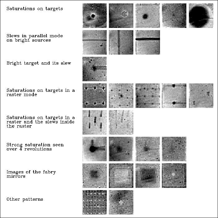
The main effect of a saturation was a decrease of the responsivity in that part of the array which had been overilluminated. This effect was manifested in science observations as an undesirable remnant of any bright source, appearing as a hole compared to the level of the neighbouring background. If no curing of the detector was performed after a saturation event, as was usually the case during ISO operations because of the time constraints, the remnant was observed for a long time after the triggering event. It could take hours or even days for the affected pixels to recover their nominal responsivity. As the effect of the decrease of the responsivity could be observed when the detector was `homogeneously' illuminated, flat-field measurements, such as those performed during the de-activation sequence, were well suited in identifying any serious event which could have occurred inside the revolution and which could have left a trace on the detector. Figure 2.4 gives an example of a gallery of patterns seen in the ICD measurements. The origin of the pattern is indicated in each case.
The on-board readout electronics had 32 independent channels, one for
each column of the array. It was based on DC amplifiers followed by
sample and hold circuitry. An analogue multiplexer was used to read each
line and to encode the signal on 4096 levels. A programmable offset was
applied before the analogue to digital converter, and the gain of the
chain could be selected from among the 3 factors: 1, 2 or
4, to allow for a good sampling of the noise in low flux
conditions, and to take advantage of the whole dynamic range. For general
user applications the
offset was automatically set, and the observer had to choose the gain; in
typical conditions, a gain of 2 was selected, providing 120
e![]() /ADU and a good sampling of the 1.5 ADU rms of the readout noise
over the whole linear range of the array. With this gain, the dynamic range
of the system was limited by the analogue to digital converter to
/ADU and a good sampling of the 1.5 ADU rms of the readout noise
over the whole linear range of the array. With this gain, the dynamic range
of the system was limited by the analogue to digital converter to
![]() 5
5![]() e
e![]() /pixel. In case of a higher signal, a gain
of 1 could be selected. Gain 4 was deprecated as it easily led to
saturations of the detector, even upon the occurence of moderate glitches.
/pixel. In case of a higher signal, a gain
of 1 could be selected. Gain 4 was deprecated as it easily led to
saturations of the detector, even upon the occurence of moderate glitches.
Column 24 of the LW detector was disconnected. The detector was still active but there was no data available. As the orientation of column 24 on the sky (which varied as a function of satellite revolution) was known only after the observations were scheduled, it was recommended for cases where data was needed across the whole array, to execute raster observations with redundant sky coverage (using a maximum raster-step size of 23 times the pfov in the y-direction). Column 24 ran in the satellite z-direction and was offset from the center of the array in the satellite y-direction (see the ISO Handbook Volume I, [40]).