The LWS used photoconductive detectors which could provide background photon noise limited sensitivies when operated at the available temperatures in ISO. An understanding of the operation of these devices is important as any non-ideal characteristics will affect the data interpretation.
In a semiconductor at very low temperatures, the electrons fill the
valence band. If the energy of a photon (wavelength ![]() )
incident on a photoconductor is greater than or equal to the energy
gap (
)
incident on a photoconductor is greater than or equal to the energy
gap (
![]() ) between the valence band and the acceptor states,
then an electron can be promoted to the acceptor states (and thus a hole
is available for conductivity). Hence for an electron to be excited:
) between the valence band and the acceptor states,
then an electron can be promoted to the acceptor states (and thus a hole
is available for conductivity). Hence for an electron to be excited:
where ![]() is Planck's constant and
is Planck's constant and ![]() is the speed of light.
If the photon's energy is not as large as the energy gap then the
photon cannot be absorbed; the material is transparent.
This produces a limit on the longest wavelength detectable.
is the speed of light.
If the photon's energy is not as large as the energy gap then the
photon cannot be absorbed; the material is transparent.
This produces a limit on the longest wavelength detectable.
By applying an electric field across a small cuboid of
photoconductive material the conduction electrons will move towards
the positive potential thus creating a small current in the external
circuit. By measuring this current the number of photons falling on
the detector can be determined.
In an intrinsic semiconductor, electrons are excited from the valence
band to the conduction band. Doping a
semiconductor produces smaller energy gaps in the detector and hence
the wavelength range of the detector can be extended.
Doped semiconductors are extrinsic and come in two types, ![]() and
and ![]() .
In
.
In ![]() type semiconductors, a substituted impurity atom in the lattice
structure donates an electron which is loosely bound to this positive
impurity centre.
For a uniformly doped device we therefore get energy levels just
below the conduction band, called donor impurity levels. Bound
electrons in these levels are promoted to the conduction band by the
absorption of an appropriate long wavelength infrared (IR) photon
because of the now much reduced band gap.
For
type semiconductors, a substituted impurity atom in the lattice
structure donates an electron which is loosely bound to this positive
impurity centre.
For a uniformly doped device we therefore get energy levels just
below the conduction band, called donor impurity levels. Bound
electrons in these levels are promoted to the conduction band by the
absorption of an appropriate long wavelength infrared (IR) photon
because of the now much reduced band gap.
For ![]() type semiconductors, the substituted impurity atom accepts an
electron, thus effectively creating a hole loosely bound to the
negative impurity centre. This creates energy levels just above the
valence band called acceptor states. When an IR photon is absorbed, an
electron from the valence band is promoted into this acceptor level
but is still bound.
This however leaves a free positive hole in the valence band which
will, with the aid of an electric field across the detector, migrate
towards the negative potential and thus produce a current.
A good description of the physics and range of available
photodetectors is given by Bratt 1977, [2].
The LWS photoconductors are all
type semiconductors, the substituted impurity atom accepts an
electron, thus effectively creating a hole loosely bound to the
negative impurity centre. This creates energy levels just above the
valence band called acceptor states. When an IR photon is absorbed, an
electron from the valence band is promoted into this acceptor level
but is still bound.
This however leaves a free positive hole in the valence band which
will, with the aid of an electric field across the detector, migrate
towards the negative potential and thus produce a current.
A good description of the physics and range of available
photodetectors is given by Bratt 1977, [2].
The LWS photoconductors are all ![]() type. The long wavelength cut-off, as
indicated in Equation 2.10, for Germanium doped with
Gallium (Ge:Ga) detectors is at 115
type. The long wavelength cut-off, as
indicated in Equation 2.10, for Germanium doped with
Gallium (Ge:Ga) detectors is at 115![]() m. Until recently, Ge:Ga
photodetectors represented the longest wavelength sensitive photodetectors
available. However, it was found that by putting the detector
under mechanical uniaxial stress the band gap could be
effectively decreased, affording detection out to just beyond
200
m. Until recently, Ge:Ga
photodetectors represented the longest wavelength sensitive photodetectors
available. However, it was found that by putting the detector
under mechanical uniaxial stress the band gap could be
effectively decreased, affording detection out to just beyond
200![]() m (see for example Wang et al. 1987, [45]).
Hence, the four longest wavelength channels in the LWS (LW2-LW5) are
all stressed.
m (see for example Wang et al. 1987, [45]).
Hence, the four longest wavelength channels in the LWS (LW2-LW5) are
all stressed.
The LWS detector sub-system, shown in Figure 2.11, had
three types of detectors: the shortest wavelength detector (43-50![]() m),
denoted SW1, was a germanium doped with beryllium detector, Ge:Be;
detectors SW2, SW3, SW4, SW5 and LW1 were unstressed germanium doped
with gallium, Ge:Ga(u), covering the total wavelength range of
50-110
m),
denoted SW1, was a germanium doped with beryllium detector, Ge:Be;
detectors SW2, SW3, SW4, SW5 and LW1 were unstressed germanium doped
with gallium, Ge:Ga(u), covering the total wavelength range of
50-110![]() m; the long wavelength detectors, LW2-5, encompassed
the range of 110-197
m; the long wavelength detectors, LW2-5, encompassed
the range of 110-197![]() m and were stressed germanium doped
with gallium, Ge:Ga(s). Figure 2.7
showed the spectral response of these detectors. SW1 had a bias
voltage of 600mV, SW2 had a bias of 200mV. The other
Ge:Ga(u) detectors had a bias voltage of 150mV. LW2 and LW5 had the
lowest bias voltages, at 40mV, and the LW3 and LW4 values were 60mV;
this information is given in full in Table 2.3.
Each detector was a 1mm sided cube.
m and were stressed germanium doped
with gallium, Ge:Ga(s). Figure 2.7
showed the spectral response of these detectors. SW1 had a bias
voltage of 600mV, SW2 had a bias of 200mV. The other
Ge:Ga(u) detectors had a bias voltage of 150mV. LW2 and LW5 had the
lowest bias voltages, at 40mV, and the LW3 and LW4 values were 60mV;
this information is given in full in Table 2.3.
Each detector was a 1mm sided cube.
| Detector | Type | Wavelength | In-orbit Bias |
| Range [ |
Voltage [mV] | ||
| SW1 | Ge:Be | 43-50.5 | 600 (500 prior to rev.191) |
| SW2 | Ge:Ga(u) | 49.5-64 | 200 (150 prior to rev.191) |
| SW3 | Ge:Ga(u) | 57-70 | 150 |
| SW4 | Ge:Ga(u) | 67-82 | 150 |
| SW5 | Ge:Ga(u) | 76-93 | 150 |
| LW1 | Ge:Ga(u) | 84-110 | 150 |
| LW2 | Ge:Ga(s) | 103-128 | 40 |
| LW3 | Ge:Ga(s) | 123-152 | 60 |
| LW4 | Ge:Ga(s) | 142-171 | 60 |
| LW5 | Ge:Ga(s) | 161-197 | 40 |
| Detector type | Ge:Be (SW1) | Ge:Ga(u) (SW2-LW1) | Ge:Ga(s) (LW2-LW5) |
| Level | |||
| 0 | 0 | 0 | 0 |
| 1 | 250 | 50 | 25 |
| 2 | 400 | 100 | 40 |
| 3 | 500 | 150 | 60 |
| 4 | 600 | 200 | 70 |
| 5 | 700 | 250 | 80 |
| 1000 | 300 | ||
| bias boost | 2V | 1V | 0.2V |
| bias boost | 3V | 2V | 0.4V |
Each detector was mounted in an integrating cavity to increase its absorption efficiency and is fed by a horn designed to couple efficiently with the radiation leaving the spherical mirror (8 of Figure 2.1).
The reduction in the energy band gap produced by a screw stressing the
detectors, also makes them more sensitive to residual thermal energy,
as the phonons can have enough energy to excite carriers into the
acceptor states. This produces a larger dark current than in an
unstressed detector. Under very low photon backgrounds, shot noise
from this dark current limits the inherent sensitivity of these devices.
The free carrier number density drops exponentially with temperature
(the Boltzmann distribution is proportional to
![]() ), so
cooling the detectors below 3K quickly reduces the number of
thermally excited carriers and hence the dark current. It was found
empirically (Church 1993, [8]) that by reducing the
temperature of the
stressed detectors to the lowest available temperature on board ISO,
which was that of the helium tank at 1.8K, the dark current could be
reduced to an acceptable level. However, it was found that when the
unstressed detectors were operated at temperatures less than 2.5K
the detectors would become unstable and spontaneously spike.
This spiking increased in severity as the temperature was reduced to
1.8K, making the detectors unusable (Church 1993,
[8]). This spontaneous spiking phenomenon is
thought (Teitsworth, Westervelt & Haller 1983,
[43]; Teitsworth & Westervelt 1986,
[42]) to be caused by trapped space charge
near the injecting contact causing local electric field breakdown
within the detector with a subsequent `avalanche' of carriers. It is due
to this spiking that the unstressed detectors (Ge:Be and Ge:Ga) are
cooled only to 3.0K, and not to 1.8K as the stressed detectors,
causing the mounting to be more complicated. At 3.0K the detectors
can be operated nearly as well as at 1.8K because the dark
current is only a factor of
), so
cooling the detectors below 3K quickly reduces the number of
thermally excited carriers and hence the dark current. It was found
empirically (Church 1993, [8]) that by reducing the
temperature of the
stressed detectors to the lowest available temperature on board ISO,
which was that of the helium tank at 1.8K, the dark current could be
reduced to an acceptable level. However, it was found that when the
unstressed detectors were operated at temperatures less than 2.5K
the detectors would become unstable and spontaneously spike.
This spiking increased in severity as the temperature was reduced to
1.8K, making the detectors unusable (Church 1993,
[8]). This spontaneous spiking phenomenon is
thought (Teitsworth, Westervelt & Haller 1983,
[43]; Teitsworth & Westervelt 1986,
[42]) to be caused by trapped space charge
near the injecting contact causing local electric field breakdown
within the detector with a subsequent `avalanche' of carriers. It is due
to this spiking that the unstressed detectors (Ge:Be and Ge:Ga) are
cooled only to 3.0K, and not to 1.8K as the stressed detectors,
causing the mounting to be more complicated. At 3.0K the detectors
can be operated nearly as well as at 1.8K because the dark
current is only a factor of ![]() 3 higher
(Church 1993, [8]).
Operating the two types of detectors at different temperatures was
achieved by mounting them on separate bars. The unstressed detectors
were mounted on the upper bar, which acommodated a heater and a
thermometer operating in a servo loop and it had a weak thermal link
to the lower bar. The stressed detectors were attached to this lower
bar, which was thermally shorted to the helium tank with a
high-conductance copper strap.
3 higher
(Church 1993, [8]).
Operating the two types of detectors at different temperatures was
achieved by mounting them on separate bars. The unstressed detectors
were mounted on the upper bar, which acommodated a heater and a
thermometer operating in a servo loop and it had a weak thermal link
to the lower bar. The stressed detectors were attached to this lower
bar, which was thermally shorted to the helium tank with a
high-conductance copper strap.
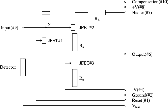
Each of the ten LWS detectors was read out by an integrating amplifier. This choice of readout was dictated by the very high impedance of the detectors under the ultra-low photon backgrounds experienced in flight, see Price 1993, [35] and Leeks 2000, [24] for more details. An integrating amplifier is, in principle, a resistor capacitor (RC) circuit. The readout circuit is shown in Figure 2.12. The voltage across the resistor in response to an input is given by:
where ![]() is the voltage supply,
is the voltage supply, ![]() the time of build up of the
voltage
the time of build up of the
voltage ![]() on
the capacitor,
on
the capacitor, ![]() is the
resistance and
is the
resistance and ![]() is the capacitance.
For
is the capacitance.
For ![]() then, expanding the exponential to first order,
Equation 2.11 becomes:
then, expanding the exponential to first order,
Equation 2.11 becomes:
| (2.12) |
and differentiating with respect to ![]() gives:
gives:
| (2.13) |
so by measuring the voltage build up in a known capacitor, the current
![]() can be recovered. This is the essence of the Infrared Labs. JF4
integrating amplifier as used in the LWS.
can be recovered. This is the essence of the Infrared Labs. JF4
integrating amplifier as used in the LWS.
For a photoconductor under low photon flux, the photon noise is
negligible so the dominant
noise processes are
Generation-Recombination (GR) noise [rms noise current,
![]() ] and electron shot noise [rms noise current,
] and electron shot noise [rms noise current,
![]() ] for a post
detection bandwidth of 1Hz. Here
] for a post
detection bandwidth of 1Hz. Here ![]() is the total current flowing in
the detector circuit,
is the total current flowing in
the detector circuit, ![]() is the electronic charge and
is the electronic charge and ![]() is the
photoconductive gain (see Bratt 1977, [2] for a detailed
description).
Since these two mechanisms are
uncorrelated the total noise current is given by their quadratic sum:
is the
photoconductive gain (see Bratt 1977, [2] for a detailed
description).
Since these two mechanisms are
uncorrelated the total noise current is given by their quadratic sum:
| (2.14) |
where ![]() is known as the dark current (the current flowing in the
absence of photons).
is known as the dark current (the current flowing in the
absence of photons).
For the LWS the average photoconductive gain, ![]() , is 0.66 (see
Table 4 of Swinyard et al. 2000, [41] for the
individual values of
, is 0.66 (see
Table 4 of Swinyard et al. 2000, [41] for the
individual values of ![]() ), giving
), giving
![]() . The responsivity for the detector circuit,
. The responsivity for the detector circuit,
![]() , gives the current,
, gives the current, ![]() , which flows in the detector when
illuminated by an infrared signal of power
, which flows in the detector when
illuminated by an infrared signal of power ![]() , such that:
, such that:
where ![]() is the Responsive Quantum Efficiency,
is the Responsive Quantum Efficiency, ![]() is Planck's
constant,
is Planck's
constant, ![]() is the speed of light and
is the speed of light and ![]() is the charge on one electron.
The NEP (
is the charge on one electron.
The NEP (![]() ) is then:
) is then:
| (2.16) |
Hence for dark currents of ![]() 100 electrons/s
100 electrons/s ![]() and an
and an ![]() product of 0.1, an NEP of
product of 0.1, an NEP of
![]() 5 10
5 10![]() WHz
WHz![]() at 100
at 100![]() m is achieved.
m is achieved.
Note that the read noise of the integrating amplifier was measured to be
![]() 10 electrons regardless of the integration time, which
is significantly less than the dark current.
10 electrons regardless of the integration time, which
is significantly less than the dark current.
The integration amplifier therefore gives a photon-noise-limited performance. It is like a trans-impedance amplifier but with an infinite feedback resistance so that there is no Johnson noise from the feedback resistor to limit the performance of the detector circuit. This made the integrating amplifier very suitable for the LWS.
|
The integrating amplifiers used typically had a gain of 0.9 and a capacitance of 7.5pF. The photons incident at a detector produced a flow of charge which accumulated at the input capacitor. The voltage produced as this capacitor charges was non-destructively read out 88 times per second (sampled every 11.4ms) through the JFET#2 (see Figure 2.12). After an appropriate time this capacitor was discharged by applying a reset pulse through reset JFET#1 at the gate of JFET#2 and also applying a compensation pulse which is adjusted to neutralise any residual charge left from the reset. After the reset the build up of voltage began again. JFET#3 balances out the offset voltage of JFET#1 so that the voltage at output #6 represents that measured at the gate of JFET#2 alone.
Two different integration times (0.5s or 0.25s)
were available with the LWS; for strong signals the
output was less noisy and more non-linear hence the shorter integration
time was more suitable. Ideally, for very strong sources, the integration
time would have been reduced even further. However, the
dead-time (the time taken for the signal
to settle down after a reset) was ![]() 50ms and so
reducing the integration time to less than 250ms would have lowered the
overall on-source efficiency and given very few data points in the
ramps for statistical evaluation.
50ms and so
reducing the integration time to less than 250ms would have lowered the
overall on-source efficiency and given very few data points in the
ramps for statistical evaluation.
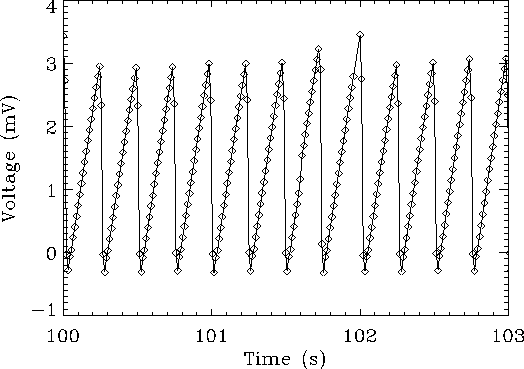
The resetting of the circuit produces a series of `ramps', where one ramp was the voltage build up between two resets representing the signal collected during the interval. Figure 2.13 shows twelve such one quarter second ramps for SW3 (22 data points per ramp; half-second ramps have 44 points). One full grating spectrum has typically 2500 ramps. The build up of charge caused a drop in the effective bias voltage (this is called de-biasing) which in turn caused a change in the responsivity. This effect was quite large in strong sources and it produced a non-linear response to the input signal. Effectively for the same increase in input the output does not increase by as much so the ramps are curved.
|
The ramps represent the incoming photon flux from the astrophysical object observed and are converted to photocurrents in the second stage of the automatic data processing (see Section 4.1).
ISO was subjected to particle hits, while in orbit about the Earth,
from energetic protons and high energy electrons.
The effect of these charged particle impacts on a detector is to generate
electron hole pairs from which the intrinsically generated electrons
neutralise the compensation donor impurities and thus increase the
mobility and hence responsivity. For laboratory dosage of high energy gammas
(60keV,
![]() 1000
1000
![]() s) it was possible to saturate the
responsivity after
s) it was possible to saturate the
responsivity after ![]() 100s, with typical observed responsivity changes
between factors of 10
and 50. Clearly any gain change of the detectors needed to be carefully
monitored if any sense was to be made of the astronomical data. The most
dramatic effect of particle hits was when passing through the Van Allen
belts.
100s, with typical observed responsivity changes
between factors of 10
and 50. Clearly any gain change of the detectors needed to be carefully
monitored if any sense was to be made of the astronomical data. The most
dramatic effect of particle hits was when passing through the Van Allen
belts.
|
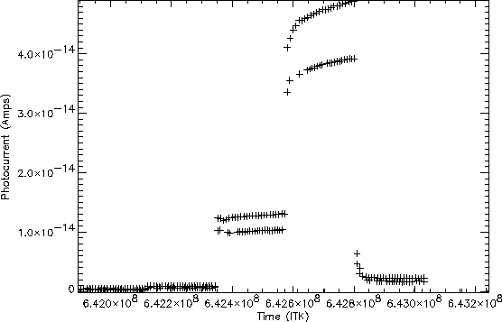
The responsivity of the detectors increased due to the particle hits: to re-normalise the responsivity, the bias current was increased to beyond the breakdown voltage for each detector. This bias boosting causes impact ionisation of the neutral impurities and therefore largely restores the pre-irradiation values of donor and acceptor levels. Operationally, bias boosting was applied on exit from the Van Allen belts. Figure 2.14 shows the reduction of the responsivity of LW4 after a second bias boost which was performed about half way through the 24 hour orbit. The data are from an illuminator flash before and after a bias boost half way through an orbit.
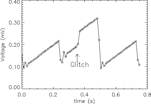
This boost was required to restore the responsivity of the detectors which also increased during the orbit as the satellite was constantly bombarded by galactic cosmic rays (H and He nuclei). However the dark currents were not affected by the cosmic rays, they remained constant during an orbit (Swinyard et al. 2000, [41]). These cosmic ray hits, about one every eight seconds, also caused the readout signal to jump (this is termed a glitch) as shown in Figure 2.15. It was found that a glitch changed the responsivity for the rest of that integration and the following ones, hence these data could not be used. The part of the integration before the glitch could, however, still be used to find the photocurrent caused by the incident photons. The longer the individual integrations, the greater the number of resets required to recover from a glitch. To reduce the number of unusable integrations, and hence the amount of observing time wasted, the length of them was reduced, from the pre-flight specification of two seconds, to one half-second (one quarter-second for strong sources, see also Section 5.7). It was then found that only two integrations after the glitched one were affected and should not be used. This still presented the high possibility of there being no good data for a particular wavelength if they were collected consecutively, hence `fast scanning' became the standard. This was where just one integration per wavelength interval was recorded and the grating was scanned to cover the required wavelength range, producing one `scan'. This was repeated to produce several scans which could be co-added.
The change in responsivity between the bias boosts was monitored by the use of IR illuminators. The five illuminators (labelled 1 to 5 in Figure 2.11), which are located in front of the detectors, output a known IR signal which is used to monitor the responsivity changes. The data of these illuminators are used to correct for the drift in responsivity with time during an orbit and an individual observation as discussed in Section 4.1.
![\resizebox {10cm}{!}{\includegraphics[120,220][475,619]{det_block.ps}}](img91.gif)